Toshiba shrinks Quantum Key Distribution into a single chip
Toshiba Europe Ltd today announced it has developed the world’s first chip-based quantum key distribution (QKD) system. This advance will enable the mass manufacture of quantum security technology, bringing its application to a much wider range of scenarios including to Internet of Things (IoT) solutions.
QKD addresses the demand for cryptography which will remain secure from attack by the supercomputers of tomorrow. In particular, a large-scale quantum computer will be able to efficiently solve the difficult mathematical problems that are the basis of the public key cryptography widely used today for secure communications and e-commerce. In contrast, the protocols used for quantum cryptography can be proven secure from first principles and will not be vulnerable to attack by a quantum computer, or indeed any computer in the future.
The QKD market is expected to grow to approximately $20 billion worldwide in FY2035. Large quantum-secured fibre networks are currently under construction in Europe and South-East Asia, and there are plans to launch satellites that can extend the networks to a global scale. In October 2020, Toshiba released two products for fibre-based QKD, which are based on discrete optical components. Together with project partners, Toshiba has implemented quantum-secured metro networks and long-distance fibre optic backbone links in the UK, Europe, US and Japan.

Manufacturing advances
For quantum cryptography to become as ubiquitous as the algorithmic cryptography we use today, it is important that the size, weight and power consumption are further reduced. This is especially true for extending QKD and quantum random number generators (QRNG) into new domains such as the last-mile connection to the customer or IoT. The development of chip-based solutions is essential to enabling mass market applications, which will be integral to the realisation of a quantum-ready economy.
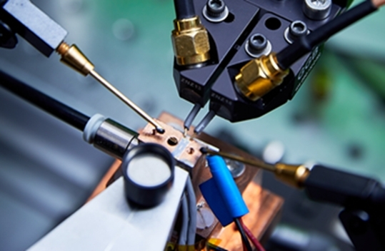
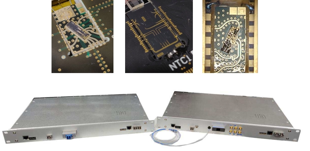
Toshiba has developed techniques for shrinking the optical circuits used for QKD and QRNG into tiny semiconductor chips. These are not only much smaller and lighter than their fibre optic counterparts, but also consume less power. Most significantly, many can be fabricated in parallel on the same semiconductor wafer using standard techniques used within the semiconductor industry, allowing them to be manufactured in much larger numbers. For example, the quantum transmitter chips developed by Toshiba measure just 2x6mm, allowing several hundred chips to be produced simultaneously on a wafer.
Andrew Shields, Head of Quantum Technology at Toshiba Europe, remarked, “Photonic integration will allow us to manufacture quantum security devices in volume in a highly repeatable fashion. It will enable the production of quantum products in a smaller form factor, and subsequently allow the roll out of QKD into a larger fraction of the telecom and datacom network.”
Taro Shimada, Corporate Senior Vice President and Chief Digital Officer of Toshiba Corporation comments: “Toshiba has invested in quantum technology R&D in the UK for over two decades. This latest advancement is highly significant, as it will allow us to manufacture and deliver QKD in much larger quantities. It is an important milestone towards our vision of building a platform for quantum-safe communications based upon ubiquitous quantum security devices.”
Part of this work was funded by the Innovate UK Collaborative R&D Project AQuaSeC, through the Industrial Strategy Challenge Fund. The details of the advancement are published in the scientific journal, Nature Photonics.

Technical Summary
QKD systems typically comprise a complex fibre-optic circuit, integrating discrete components, such as lasers, electro-optic modulators, beam-splitters and fibre couplers. As these components are relatively bulky and expensive, the purpose of this work was to develop a QKD system in which the fibre-optic circuit and devices are written in millimetre scale semiconductor chips.
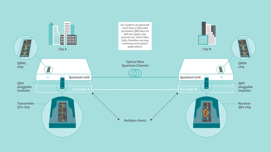
Toshiba has developed the first complete QKD prototype in which quantum photonic chips of different functionality are deployed. Random bits for preparing and measuring the qubits are produced in quantum random number generator (QRNG) chips and converted in real-time into high-speed modulation patterns for the chip-based QKD transmitter (QTx) and receiver (QRx) using field-programmable gate arrays (FPGAs). Photons are detected using fast-gated single photon detectors. Sifting, photon statistics evaluation, time synchronisation and phase stabilisation are done via a 10 Gb/s optical link between the FPGA cores, enabling autonomous operation over extended periods of time. As part of the demonstration, the chip QKD system was interfaced with a commercial encryptor, allowing secure data transfer with a bit rate up to 100 Gb/s.

To promote integration into conventional communication infrastructures, the QKD units are assembled in compact 1U rackmount cases. The QRx and QTx chips are packaged into C-form-factor-pluggable-2 (CFP2) modules, a widespread form-factor in coherent optical communications, to ensure forward compatibility of the system with successive QKD chip generations, making it easily upgradeable. Off-the-shelf 10 Gb/s small-form-factor pluggable (SFP) modules are used for the public communication channels.
Taofiq Paraiso, lead author of the Nature Photonics paper describing the chip-scale QKD system, says: “We are witnessing with photonic integrated circuits a similar revolution to that which occurred with electronic circuits. PICs are continuously serving more and more diverse applications. Of course, the requirements for quantum PICs are more stringent than for conventional applications, but this work shows that a fully deployable chip-based QKD system is now attainable, marking the end of an important challenge for quantum technologies. This opens a wide-range of perspectives for the deployment of compact, plug-and-play quantum devices that will certainly strongly impact our society.”


