Your future car could be a Radar Antenna
Radar miniaturization is one of the key trends that IDTechEx has identified in “Automotive Radar 2022-2042”. There are several factors that are contributing towards this, such as moving from 24GHz to 77GHz which shrinks the antenna size.
Or, transitioning from SiGe-BiCMOS based transceivers to Si-CMOS ones, which reduces the number of discrete computational components and shrinks the circuit board.
Multi-layer radars
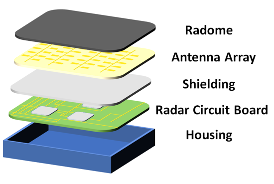
A traditional radar has several component layers stacked on top of each other, each with distinct tasks. The radome is the outer protective face, which must allow the radio waves to pass through seamlessly. The antenna array converts between an electrical signal and emitted radio waves, as well as reading radio echoes and converting back to an electrical signal. The shielding separates the antenna array and the radar circuit board, where the radar circuit board holds key components like the transceiver and processors.
Radars like this still exist, but they tend to use the increased footprint availability to pack in as much performance as possible. For example, new high-performance radars from Continental, Arbe, and others still have fairly large footprints. These radars are typically used at the front of the vehicle where high resolution and long ranges are necessary. But around the rest of the vehicle, ranges can be shorter, and precise positioning of detected objects is less important than field of view and measuring proximity.
These changes in requirements allow the size of the radar to be reduced and open up more possibilities to further reduce the package size.

Board integration
The current trend from radar suppliers such as Bosch, Continental, Infineon, and NXP is to integrate the radar circuit board and antenna. Combining these shrinks the packaging by removing the need for a shielding layer and making a separate antenna array board redundant. Part of the progress has been made by moving from 24GHz to 77GHz which results in shorter wavelength radio waves and a smaller antenna array. The second enabling factor is the move towards highly integrated chips.
Instead of having multiple discrete chips on the radar circuit board, Si-CMOS technology allows the transceiver to perform nearly all the tasks required for radar, such as signal processing and object identification. This frees up room on the radar board, making space for the antenna. Not all suppliers are jumping straight to Si-CMOS though.
Antenna on package
Some innovators and suppliers, for example, Texas Instruments, are going one step further and putting the antenna on the top of the transceiver chip itself. This means the entire radar can be reduced to just a few 10s of millimetres in each direction. This is the cutting edge of radar tech and it is hard to see how radar could get any smaller.

Antenna on vehicle
The compromise that designers must make when reducing the radar’s size is worsening performance. A smaller antenna array can have poor range and poor resolution. So, is there a way to get all the benefits of a big antenna array, while still having high levels of integration?
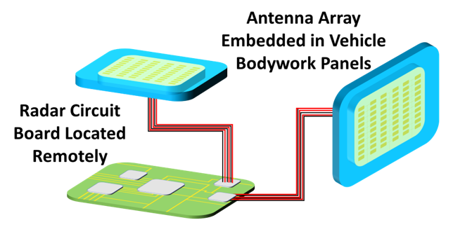
One possible solution is to start embedding the antenna in the outer surface of the vehicle. This has been proposed in research already; for example, the Fraunhofer Institute are working on RadarGlass which transforms headlights into radars. IDTechEx thinks this could also be applied to body panels, embedding the antenna in the plastic to create enormous, versatile, and powerful arrays. Additionally, by delocalizing the antenna, multiple arrays could be coordinated across a single controller. With the large antenna arrays working in unison, further performance gains might be unlocked.
A variety of additive electronics manufacturing processes could be utilized to integrate radar antennas into car body panels, or onto their surface. One of the most developed methods is laser direct structuring (LDS), which uses a laser to selectively activate an additive within an injection-moulded plastic component followed by electroless plating. This method is already used to produce antennas in a wide variety of consumer electronics devices. methods in an earlier stage of development include in-mould electronics (IME), in which the conductive traces are deposited prior to thermoforming and subsequent injection moulding, applying functionalized films with the metal pattern already printed on them, and simply printing conductive patterns on a 3D surface. The IDTechEx report “3D Electronics 2020-2030: Technologies, Forecasts, Players” offers detailed insight into how electronics can be integrated within or onto the surface of 3D structures.
There would be questions about the practicality of how this integration fits into the existing value chain though since manufacturing a radar in this way is far less straightforward than a supplier handing over a box for the OEM to fit. For example, who makes the body panels? It is unlikely that BMW and Mercedes would want their doors designed by Bosch, but at the same time how could a supplier like Bosch design a radar antenna for every single variation of door that BMW and Mercedes offer. This concept might be of interest to someone like Tesla, who have a highly vertical manufacturing process, but Tesla seems to be moving away from radar. This kind of tech is likely to be embedded in the drawing board for a little while longer.


