


Intel announces milestone in large-scale Quantum Qubit Chip Production
The Intel Labs and Components Research organizations have demonstrated the industry’s highest reported yield and uniformity to date of silicon spin qubit devices developed at Intel’s transistor research and development facility, Gordon Moore Park at Ronler Acres in Hillsboro, Oregon. This achievement represents a major milestone for scaling and working towards fabricating quantum chips on Intel’s transistor manufacturing processes.
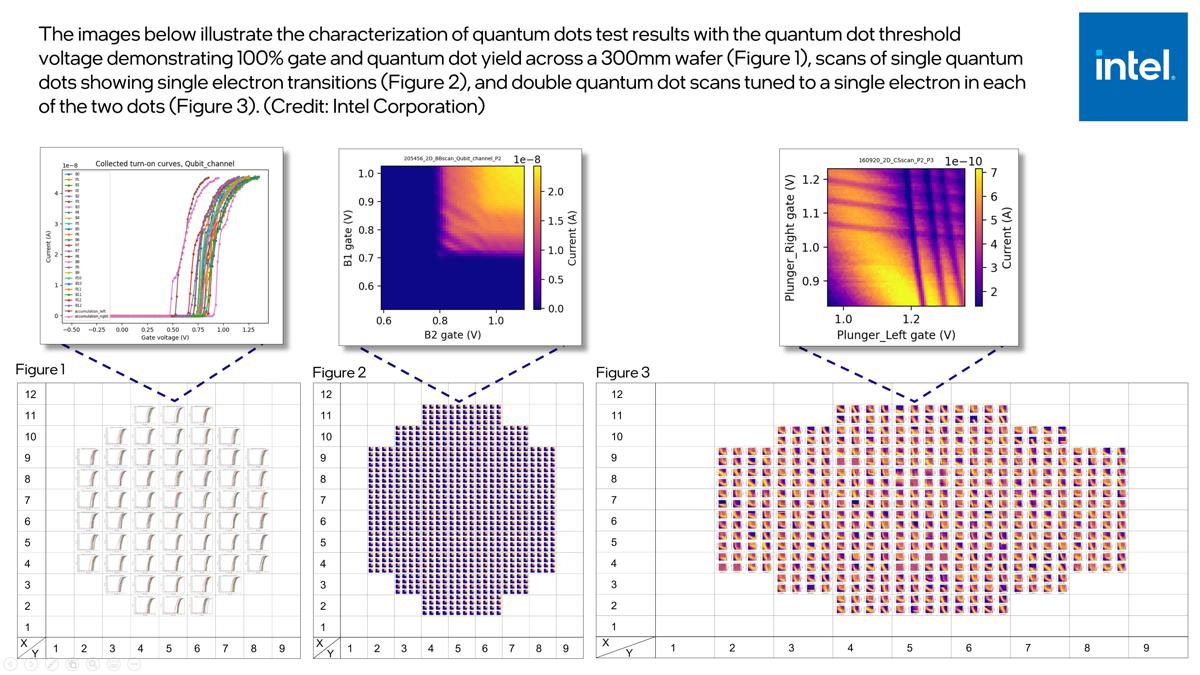
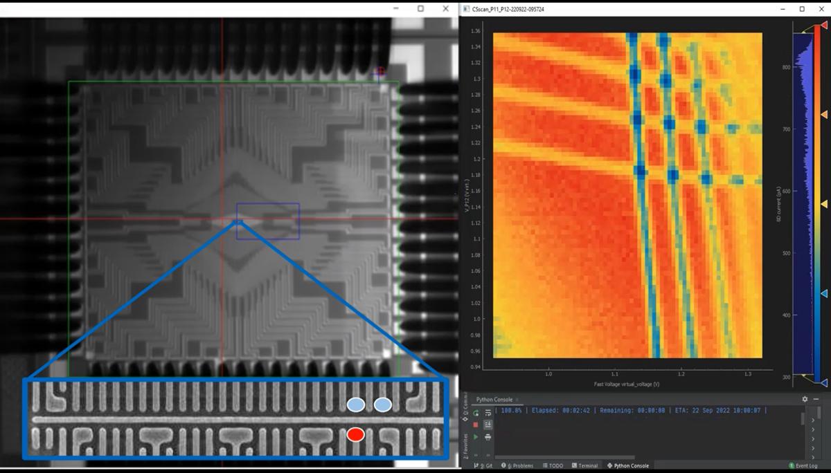
The research was conducted using Intel’s second-generation silicon spin test chip. Through testing the devices using the Intel cryoprober, a quantum dot testing device that operates at cryogenic temperatures (1.7 Kelvin or -271.45 degrees Celsius), the team isolated 12 quantum dots and four sensors. This result represents the industry’s largest silicon electron spin device with a single electron in each location across an entire 300-millimetre silicon wafer.
Today’s silicon spin qubits are typically presented on one device, whereas Intel’s research demonstrates success across an entire wafer. Fabricated using extreme ultraviolet (EUV) lithography, the chips show remarkable uniformity, with a 95% yield rate across the wafer. The use of the cryoprober together with robust software automation enabled more than 900 single quantum dots and more than 400 double dots at the last electron, which can be characterized at one degree above absolute zero in less than 24 hours.
Increased yield and uniformity in devices characterized at low temperatures over previous Intel test chips allow Intel to use statistical process control to identify areas of the fabrication process to optimize. This accelerates learning and represents a crucial step toward scaling to the thousands or potentially millions of qubits required for a commercial quantum computer.
Additionally, the cross-wafer yield enabled Intel to automate the collection of data across the wafer at the single electron regime, which enabled the largest demonstration of single and double quantum dots to date.
This increased yield and uniformity in devices characterized at low temperatures over previous Intel test chips represents a crucial step toward scaling to the thousands or potentially millions of qubits required for a commercial quantum computer.
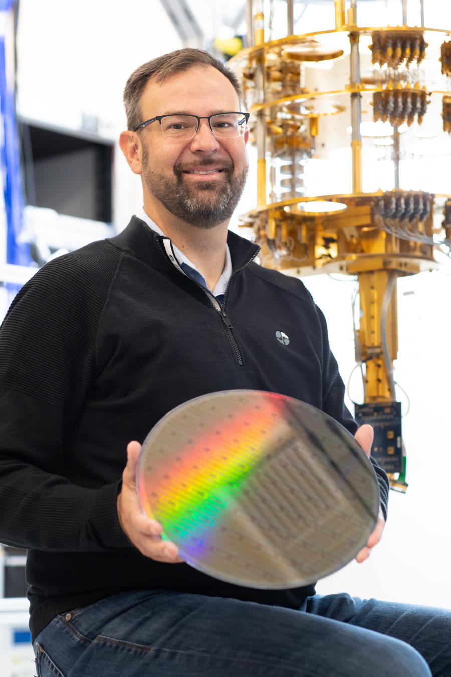
“Intel continues to make progress toward manufacturing silicon spin qubits using its own transistor manufacturing technology,” said James Clarke, director of Quantum Hardware at Intel. “The high yield and uniformity achieved show that fabricating quantum chips on Intel’s established transistor process nodes is the sound strategy and is a strong indicator for success as the technologies matures for commercialization.
“In the future, we will continue to improve the quality of these devices and develop larger scale systems, with these steps serving as building blocks to help us advance quickly,” Clarke said.