


Microelectronics to take computing to new heights
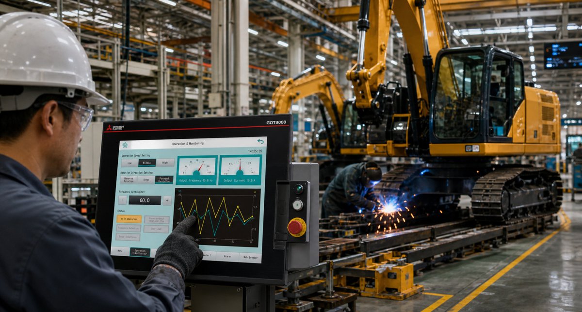
You’re seeing the story on your screen right now thanks to tiny switches known as transistors. The microchips in computers contain billions of them, each one sending electrical signals based on what you want the computer to do.
Microelectronics like these have become both essential and amazingly minuscule in the push to extract more computing power from less space. A single red blood cell dwarfs today’s average transistor, which is about a thousand times smaller.
That’s still not quite small enough.
In a future driven by data and artificial intelligence (AI), even the most “micro” of microelectronics will need to shrink further — and use less energy to boot. Scientists at the U.S. Department of Energy’s (DOE) Argonne National Laboratory are inventing the next generation of these computing building blocks.
The impact extends beyond our phones and desktops. Everything from how we travel to how we fight disease to our understanding of the universe and Earth’s climate depends on microelectronics-based devices.
“Microelectronics are so embedded in everything we do that they’re really critical to the way we run our lives these days,” said Argonne Distinguished Fellow and Materials Science Division Director Amanda Petford-Long, citing examples such as cars, online banking and the electric grid. “I don’t think anyone can get by without them.”
Pushing the limits of Moore’s law
Current microchips in smartphones can perform 17 trillion calculations per second, making them millions of times more powerful than their predecessors from several decades ago.
That astonishing leap in computing power seems unimaginable — except that someone did imagine it: engineer Gordon Moore. Moore, who went on to co-found Intel, predicted in 1965 that the number of transistors placed on microchips would double every year for the next decade. He was right, and in 1975, when the number of transistors on a microchip surpassed 65,000, he revised the pace of doubling to every two years.
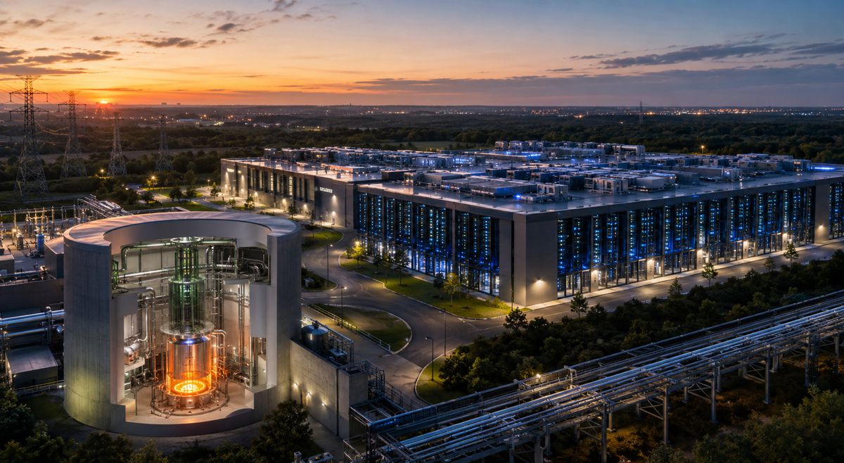
What’s now known as Moore’s law has held true, more or less. Today, a laptop might contain tens of billions of transistors embedded on a fingernail-size chip. The upcoming Aurora exascale supercomputer at the Argonne Leadership Computing Facility (ALCF), a DOE Office of Science user facility, runs on tens of thousands of state-of-the-art processors that each pack 100 billion transistors into less than 4 square inches.
The Aurora processors’ power will enable more than 2 quintillion calculations per second. Those calculations will fuel the discoveries we need to generate clean energy, fight viruses, build more efficient engines, explore space — and, of course, explore the next frontier of microelectronics, among other endeavours.
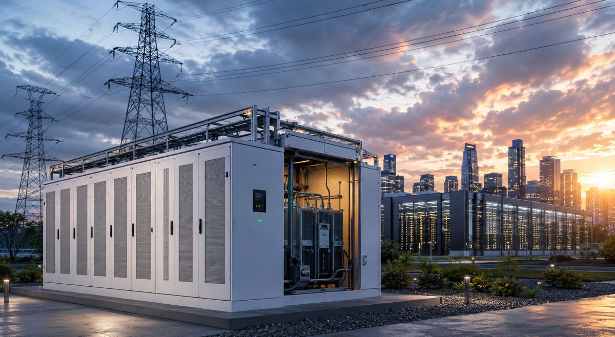
At some point, though, Moore’s law begins to run into physical barriers. Materials start to behave differently as device sizes vanish to the atomic level. Devices might trap too much heat when stacked together, and they hit walls on memory and speed. Even more pressing, our growing need for microelectronics devours energy and is projected to consume a quarter of the world’s supply by 2030.
Argonne researchers are tackling these problems through a combination of new materials, hardware and software designs, and manufacturing methods. In the process, they are also pushing the boundaries of where computers can go, making electronics that stretch like skin or operate in scorching temperatures beyond your oven’s hottest setting.
Building better materials for microelectronics
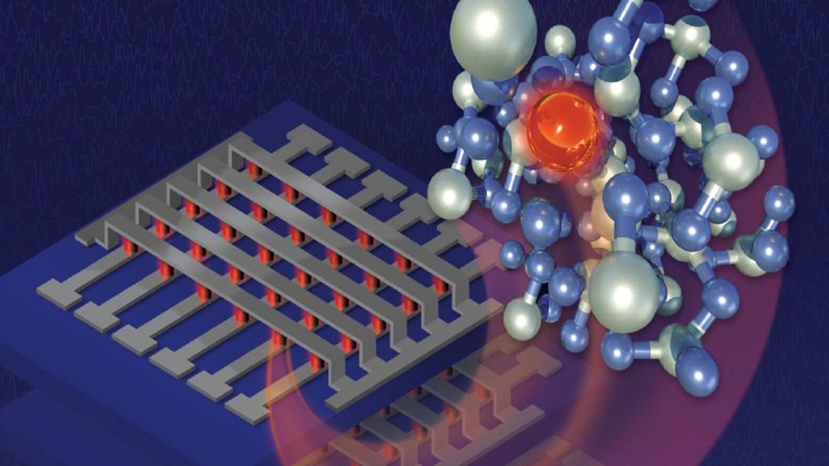
Silicon has been the workhorse material used to make each successive wave of powerful microchips. It’s abundant, and its conductivity — the ability to transmit electricity — can be adjusted by adding impurities. However, the size of microelectronics is now measured in single-digit nanometres, or a billionth of a meter. The smaller they get, the harder it is to pattern these impurities reliably.
Researchers at Argonne and other national laboratories are exploring alternative materials and designs to get around this limitation, as well as to increase energy efficiency. One possibility is to incorporate materials that have reversible responses to electric fields. Another project focuses on using metal oxides to create printable transistors. Diamond thin films are being developed using the Center for Nanoscale Materials, a DOE Office of Science user facility, to remove the heat that builds up when microelectronics are placed on top of each other.
Honing these concepts requires time-consuming steps to determine the optimal conditions for creating a particular material. Thin films, for example, are grown on surfaces atom-by-atom in a process called atomic layer deposition. Researchers use a special apparatus to make these films, evaluating conditions in cycle after cycle. It’s not unlike testing a baking recipe, where you have to wait for the final product to come out of the oven and then determine what went right or wrong before starting over again.
To move faster, researchers are experimenting with self-driving labs that bring AI into the loop. The process may start with computer simulations that inform actual experiments. The data from experiments then strengthens the simulations, and so on.
Angel Yanguas-Gil, a principal materials scientist at Argonne, is applying the self-driving lab concept to atomic layer deposition for faster, and thus lower-cost, discovery of materials for microelectronics. In this case, AI is helping to drive the experiment.
“The computer is making its own decision and exploring a new condition in real time, and then you end up with the optimum condition much faster,” said Yanguas-Gil. “It takes a matter of minutes instead of, say, days.”
Co-design for smarter microelectronics development
In a space where materials are designed down to the atom, the most ingenious innovation will have trouble moving beyond the lab if it is not fit to a specific purpose.
“We spend many years developing materials with very interesting properties, but the connection with the applications sometimes isn’t strong,” Yanguas-Gil said.
Scientists are addressing this gap in the Threadwork project. The name nods to weaving together different strands of microelectronics development with specific uses in mind, particularly those for future detectors in high energy physics and nuclear physics. Those strands include the materials, the devices built with those materials, the system architecture and more.
“In Threadwork, we’re constantly looking at all these different levels of system design and what they mean in terms of the end use,” said Mathematics and Computer Science Division Director Valerie Taylor who leads the project. “It’s not that one person’s working independently of what everybody else is doing. You’re working on designs together, from different perspectives.”
Many of these designs for microchips, along with the software they power, attempt to mimic the brain.
“The brain consists of approximately 86 billion neurons, but only uses about 20 watts of power. This is great energy efficiency,” Taylor said. “So, we are developing brain-inspired or neuromorphic devices.”
A traditional computer architecture has separate areas for operations and for memory. That layout requires information to constantly flow between the two areas, limiting how fast computers can process it. Future neuromorphic processors might be set up more like your brain, where memories and actions combine in sets of neurons that are networked together. A more compact, brain-like network reduces the amount of travel for electric signals, boosting efficiency. Transistors similar to neurons, or memristors, also might be able to communicate not just a binary value — zero or one — but a range of values within one signal, the way spikes from neurons do.
Human brains are not the only models for Argonne’s interdisciplinary design approach. Yanguas-Gil and colleagues have designed and simulated a neuromorphic chip inspired by the brains of bees, fruit flies and ants. The concept relies on a unique material developed at Argonne and was tested using the ALCF’s Theta supercomputer.
This world is not flat for long
“It sounds trivial, but one of the biggest challenges in going smaller with microelectronics is that you have to be able to make the thing,” said Petford-Long. To use another baking analogy, if you’re making a “cookie” that is 10 atoms across, it’s extremely hard to get a cookie cutter that can churn out absolutely identical shapes. Even minute variations matter, Petford-Long added: “Because these structures are so small, one inconsistency can make a big difference in how they behave.”
Another challenge is that the actual shape being stamped out may change from a flat plane with transistors in rows to more neuron-like shapes that also may be stacked on top of one another.
“Current lithography for semiconductors is highly successful, but it is set up for a 2D world where the chip is flat,” said Supratik Guha, senior advisor to Argonne’s Physical Sciences and Engineering directorate and a professor at the Pritzker School of Molecular Engineering at the University of Chicago. “In the coming decades, chips will become increasingly 3D. This requires new ways of fabricating chips.”
One of those new ways might be to use 3D printers. One Argonne project aims to create low-power, high-performance printable transistors. Other work is focused on even finer and more precise tools for atomic layer deposition that can chisel increasingly intricate features onto devices.
New ways to make tiny machines
As scientists explore new materials, configurations and manufacturing techniques for microelectronics, the Advanced Photon Source (APS), a DOE Office of Science user facility, will be key. With an upgrade that is currently in progress, the APS’s X-ray beams will become up to 500 times brighter. The increased brightness will also lend itself to smaller spot sizes that can zero in on the smallest of features in a material or semiconductor device.
The powerful new tools at Argonne will contribute to a sort of flywheel effect. The APS and other observational tools will generate more data than ever. That data will feed the innovation of the very processors that will analyse it at the Aurora supercomputer and beyond.
“Some of this work is in the very initial stages, but this is why we do continuous basic research,” Guha said. “The questions we are trying to answer will lead us to design new classes of materials and devices — and new ways of connecting them — so that, moving forward, we can meet the extreme energy efficiency challenges that we face.”
This research is funded, in part, by the DOE Office of Basic Energy Sciences and the DOE Advanced Scientific Computing Research program.