


Next-Gen Materials with Direct Observation of Electron Transfer in Solids
Nanoscale electron transfer (ET) in solids is fundamental to the development of multifunctional materials. However, ET in solids is not yet clearly understood.
Now, researchers from Japan achieved a direct observation of solid-state ET through X-ray crystal analysis by fabricating a novel double-walled non-covalent crystalline nanotube, which can absorb electron donor molecules and maintain its crystalline structure during ET. This innovative approach can lead to the design of novel functional materials soon.
Electron transfer (ET) is a process in which an electron is transferred from one atom or molecule to another. ET is fundamental to electrochemical reactions with applications in many fields. Nanoscale ET, which involves the transfer of electrons in the range of 1–100 nanometres in solids is fundamental to the design of multifunctional materials. However, this process is not yet clearly understood.
Nanotubes, nanomaterials with unique cylindrical nanostructures, offer a variety of ET properties that can be realized through electron and hole (vacant spaces left by electrons) injections into the nanotubes, making them a suitable candidate for studying nanoscale ET. Although carbon-based nanotubes have fascinating ET properties, they are particularly difficult to control in terms of their shape and size due to extreme conditions, such as high temperatures, required for their synthesis.
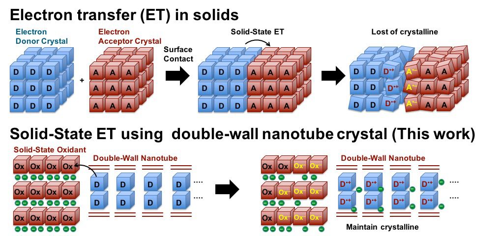
A viable approach for fabricating well-defined tuneable nanotubes is bottom-up fabrication of non-covalent nanotubes, which sometimes result in crystalline-form nanotubes. Non-covalent nanotubes are formed through the inherent attractive interactions or non-covalent interactions between atoms, instead of the strong covalent interactions seen in carbon nanotubes. However, they are not strong enough to endure electron and hole injections, which can break their non-covalent interactions and destroy their crystalline structure.
In a recent study, a team of researchers from the Department of Applied Chemistry at Tokyo University of Science, led by Professor Junpei Yuasa and including Dr. Daiji Ogata, Mr. Shota Koide, and Mr. Hiroyuki Kishi, used a novel approach to directly observe solid-state ET. Prof. Yuasa, explains: “We have developed crystalline nanotubes with a special double-walled structure. By incorporating electron donor molecules into the pores of these crystalline nanotubes through a solid-state oxidation reaction, we succeeded in directly observing the electron transfer reaction in the solid using X-ray crystal structure analysis.”
Their findings were published in the journal Nature Communications on May 23, 2024.
The researchers used a novel supramolecular crystallization method, which involves oxidation-based crystallization, to fabricate zinc-based double-walled crystalline nanotubes. This double-walled structure with large windows in the nano-tube walls makes the crystal robust and flexible enough to maintain its crystalline state when subjected to ET oxidation processes. Moreover, this structure allows the crystal to absorb electron donor molecules.
The researchers used ferrocene and tetrathiafulvalene as electron donor molecules, which were absorbed through the windows of the nanotube crystals. This allows electrons to be removed from the absorbed electron donors through solid-state ET oxidation reactions, resulting in the accumulation of holes in the donors inside the nanotube. Due to the robustness of the crystals, the researchers were able to observe this ET oxidation process using X-ray crystal structure analysis directly, uncovering key insights.
This novel approach is highly valuable for direct observation of ET in solid nanomaterials. Highlighting the potential applications of this study, Prof. Yuasa, says: “Understanding ET can lead to the development of novel functional materials, which in turn can lead to the design of more efficient semiconductors, transistors, and other electronic devices. Optoelectronic devices, such as solar cells, rely heavily on ET. Hence, direct observation of ET can help improve these devices’ performance. Additionally, this approach can lead to advancements in energy storage, nanotechnology, and materials science research.”
Overall, this study is a striking example of direct observation of solid-state ET, which can be expanded to observe ET and related phenomena in other nanomaterials.