Twisting 2D materials may lead to improved electronic and optical devices
A new generation of electronics and optoelectronics may soon be possible by controlling twist angles in a particular type of bilayer 2D material used in these devices, strengthening the intrinsic electric charge that exists between the two layers, according to researchers from Penn State, Harvard University, Massachusetts Institute of Technology and Rutgers University.
The researchers worked with regular transition metal dichalcogenides (TMD) 2D materials and Janus TMDs, a class of 2D materials named after the Roman god of duality, Janus. These bilayer 2D materials have an interaction between layers known as a van der Waals interlayer coupling that leads to a charge transfer, a process important to the functionality of electronic devices. The charge transfer for both sides of conventional TMDs is the same due to each side having the same type of atoms. In the case of Janus TMD materials, the atoms on each side of the material are different types, leading to varied charge transfer when each side is in contact with other 2D materials.
“In our study, the two types of atoms on each side of the Janus TMD material were sulfur and selenium,” said Shengxi Huang, assistant professor of electrical engineering and biomedical engineering at Penn State and co-author of the study recently published in ACS Nano. “Because they are different, there can be a charge separation or charge imbalance for the top and bottom side. It creates a vertically directed intrinsic electric field that is very different from conventional 2D materials.”
In previous research, Huang and the other researchers worked to understand whether this intrinsic electric field would impact adjacent 2D materials when they are layered. They found that the coupling is stronger in the Janus 2D materials than traditional 2D materials, due to the asymmetric charge caused by the different types of atoms on each side.
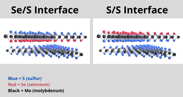
For the current work, they manually stacked two types of material layers, Janus TMD and regular 2D materials, which caused random angles depending on how they were stacked. But when they tuned the angles of how each layer was stacked to specific degrees, they made an interesting finding. If the triangle-shaped materials are twisted to stack at a zero-degree angle, when they are perfectly aligned, or at a 60-degree angle, when they are the exact opposite of perfect alignment, they found the couplings to be much stronger than at random angles. In addition, they also found the interlayer coupling is stronger when the Janus TMD is layered on the conventional TMD with the same type of element.
“The main finding was that for this same sulfur/sulfur interface, the interlayer coupling is much stronger than the sulfur/selenium interface,” Huang said. “And this is because of the charge distribution related to the dipole direction in these atoms. This means there can be an effective charge transfer between the two layers. Based on our calculation, the separation, meaning the distance between the interlayers, is much smaller, so that shows there’s a stronger coupling.”
To discover this, Huang and the team used low-frequency Raman spectroscopy. They shone light onto the two layers of 2D materials, which caused the materials’ atoms to vibrate. If the vibration is faster and at higher frequency, that indicates the interlayer coupling is strong.
“You can imagine this using a spring connecting two balls,” Huang said. “If the spring is vibrating really fast, that means this spring is strong.”
The other method that the team used during its research was photoluminescence spectroscopy. When two layers of 2D material exchange charges between each other, the light emission intensity in one of the materials will drop. This is because there are some charges that transfer to the other layer, and there’s not enough charge for the photoluminescence to happen in the “sending” layer.
“We used this as a measure of the degree of charge transfer between the two layers,” said Kunyan Zhang, doctoral candidate in electrical engineering at Penn State and co-lead author in the study. “These results we got from the light emission are consistent with our low-frequency Raman spectroscopy. Where we see a stronger coupling from the atomic vibration, we also see a larger drop in the light emission.”
These findings are important for the advancement of electronics and optoelectronics. Controlling the interlayer coupling and inducing different optical and/or electronic behaviours has great importance for the performance of many optoelectronic and electronic devices.
“These new material abilities can affect lots of applications, ranging from optoelectronics to electronic devices to catalytic abilities in electrochemical devices such as batteries,” Huang said. “These devices are all over in our everyday lives, such as lighting, electronics, appliances and batteries.”
Continued work in this research realm will include how the interlayer coupling affects other types of materials. In addition, their findings may be of use to other researchers in the future.
“People outside our field could benefit from our study,” Zhang said. “Tuning this kind of interior coupling using the interface with twist angles was not studied before. Those findings may be striking for others in the 2D field whose work does not involve Janus TMDs.”
Along with Huang and Zhang, other researchers in the study include from the Massachusetts Institute of Technology co-lead authors Yunfan Guo, postdoctoral fellow in electrical engineering, and Jing Kong, professor of electrical engineering. From Harvard University, researchers in the study include Daniel T. Larson, postdoctoral fellow in physics; Ziyan Zhu, doctoral student in physics; and Efthimios Kaxiras, John Hasbrouck Van Vleck Professor of Pure and Applied Physics and chair of the Harvard Department of Physics. An additional author in the study is Shiang Fang, postdoctoral associate in physics at Rutgers University.

The National Science Foundation and U.S. Department of Energy supported this research.


