


Making new Crystalline Materials with two or more elements
Argonne National Laboratory scientists have found a new way to make materials for batteries, magnets and microelectronics.
The world’s best artists can take a handful of differently coloured paints and create a museum-worthy canvas that looks like nothing else. They do so by drawing upon inspiration, knowledge of what’s been done in the past and design rules they learned after years in the studio.
Chemists work in a similar way when inventing new compounds. Researchers at the U.S. Department of Energy’s (DOE) Argonne National Laboratory, Northwestern University and The University of Chicago have developed a new method for discovering and making new crystalline materials with two or more elements.
“We expect that our work will prove extremely valuable to the chemistry, materials and condensed matter communities for synthesizing new and currently unpredictable materials with exotic properties,” said Mercouri Kanatzidis, a chemistry professor at Northwestern with a joint appointment at Argonne.
“Our invention method grew out of research on unconventional superconductors,” said Xiuquan Zhou, a postdoc at Argonne and first author of the paper. “These are solids with two or more elements, at least one of which is not a metal. And they cease to resist the passage of electricity at different temperatures — anywhere from colder than outer space to that in my office.”
Over the last five decades, scientists have discovered and made many unconventional superconductors with surprising magnetic and electrical properties. Such materials have a wide gamut of possible applications, such as improved power generation, energy transmission and high-speed transportation. They also have the potential for incorporation into future particle accelerators, magnetic resonance imaging systems, quantum computers and energy-efficient microelectronics.
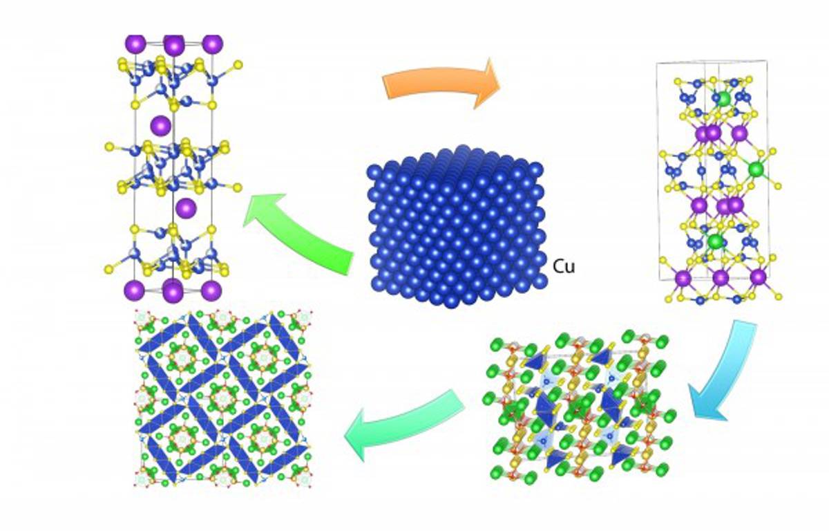
The team’s invention method starts with a solution made of two components. One is a highly effective solvent. It dissolves and reacts with any solids added to the solution. The other is not as good a solvent. But it is there for tuning the reaction to produce a new solid upon addition of different elements. This tuning involves changing the ratio of the two components and the temperature. Here, the temperature is quite high, from 750 to 1,300 degrees Fahrenheit.
“We are not concerned with making known materials better but with discovering materials no one knew about or theorists imagined even existed,” Kanatzidis noted. “With this method, we can avoid reaction pathways to known materials and follow new paths into the unknown and unpredicted.”
As a test case, the researchers applied their method to crystalline compounds made of three to five elements. As recently reported in Nature, their discovery method yielded 30 previously unknown compounds. Ten of them have structures never seen before.
The team prepared single crystals of some of these new compounds and characterized their structures at UChicago’s ChemMatCARS beamline at 15-ID-D and the X-ray Science Division’s 17-BM-B of the Advanced Photon Source, a DOE Office of Science user facility at Argonne. “With beamline 17-BM-B of the APS, we were able to track the evolution of the structures for the different chemical phases that formed during the reaction process,” said 17-BM-B beamline scientist Wenqian Xu.
“Traditionally, chemists have invented and made new materials relying only on knowledge of the starting ingredients and final product,” Zhou said. “The APS data allowed us to also take into account the intermediate products that form during a reaction.”
The Center for Nanoscale Materials, another DOE Office of Science user facility at Argonne, contributed key experimental data and theoretical calculations to the project.
And this is only the beginning of what is possible, since the method can be applied to almost any crystalline solid. It can also be applied to producing many different crystal structures. That includes multiple stacked layers, a single layer an atom thick and chains of molecules that are not linked. Such unusual structures have different properties and are key to developing next-generation materials applicable to not only superconductors, but also microelectronics, batteries, magnets and more.
This research was supported by the DOE’s Office of Science, Basic Energy Sciences program.
The associated Nature paper is titled “Discovery of chalcogenides structures and compositions using mixed fluxes.” Besides Zhou, Kanatzidis and Xu, authors include C. V. S. Kolluru, L. Wang, T. Chang, Y.-S. Chen, L. Yu, J. Wen, M. K. Y. Chan and D.-Y. Chung.