


Nanoscale Electron Imaging reveals how Heat Moves in Materials
Scientists develop a nanoscale electron imaging method that reveals the dynamics of the collective vibrations of atoms at the interface between materials.
In crystals, atoms vibrate around their equilibrium, or basic, positions. The vibration of all the atoms in a crystal forms collective modes called “phonons.” Measuring the phonon properties of nanostructures and the interfaces between materials provides insights into how well heat moves from one material to another.
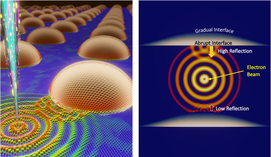
Researchers used energetic electrons to excite phonons and probe their movement. The scientists developed a novel technique to map how the momentum of phonons changes. The map reveals the direction of phonon propagation and thus the direction of heat flow on the nanoscale.
This research demonstrates that an abrupt boundary between different materials tends to reflect heat much more efficiently than a gradual, diffuse boundary.
Heat can be converted to electricity using materials called thermoelectrics. Thermoelectrics use defects in their crystal materials to slow the movement of heat. This improves the efficiency with which the materials convert heat to electricity. However, scientists’ ability to engineer devices that span a few nanometres has outpaced their understanding of the inner workings of these materials.
Scientists need to understand how heat moves at the nanoscale to advance the fields of energy conversion, quantum computing, and nanotechnology in general. This new research provides insights into how well heat is transported from one material to another.
This information can help researchers tailor thermoelectric properties on the nanoscale and to design more advanced nanodevices.
As industry has miniaturized electronic, thermoelectric, and computer technologies to nanometre scale, researchers have faced the challenge of how to study the fundamental thermal properties of the materials involved. Electron microscopy has a tremendous advantage over traditional methods due to its ability to resolve atoms. Now electron microscopy is capable of probing vibrational information at the atomic scale.
In this study, scientists developed and implemented cutting-edge monochromated electron energy-loss spectroscopic methods in a transmission electron microscope to map lattice vibrations (phonons) at atomic resolution, enabling deeper understanding of the way heat travels through nanostructured quantum dot superlattices.
The team investigated stacked silicon germanium alloy quantum dots separated by silicon and discovered that vibrations were being softened in the quantum dot due to the strain built within the nanostructure. The softening of vibrations is behind one of the many mechanisms of how thermoelectrics impede the flow of heat. More notably, the researchers developed a novel technique that can map the direction the thermal carriers, phonons, are traveling.
They found that the more atomically sharp the interface between the quantum dot and the surrounding silicon is, the more effectively the phonons are reflected. Conversely, if the composition change from quantum dot to silicon is more gradual, far fewer phonons are reflected.
This work not only demonstrates the viability of vibrational spectroscopy in the electron microscope for the field of thermoelectrics, but also provides a physical foundation for their targeting engineering.
The research was supported primarily by the Department of Energy Office of Science, Office of Basic Energy Sciences, Division of Materials Sciences and Engineering, and partially by the National Science Foundation.