


Flexible Hybrid Electronics set to drive innovation and opportunities
While flexible electronics have been around for years, either as flexible PCBs or genuinely printed electronics, there has always been a trade-off between flexibility and capability. Circuits with a few printed transistors based on organic semiconductors could be printed onto flexible substrates but were not generally capable of significant data processing.
On the other hand, thanks to adherence with Moore’s law, very capable silicon ICs (integrated circuits) are incredibly cheap on a per transistor basis but impose a rigid form factor and require careful placement onto a substrate.
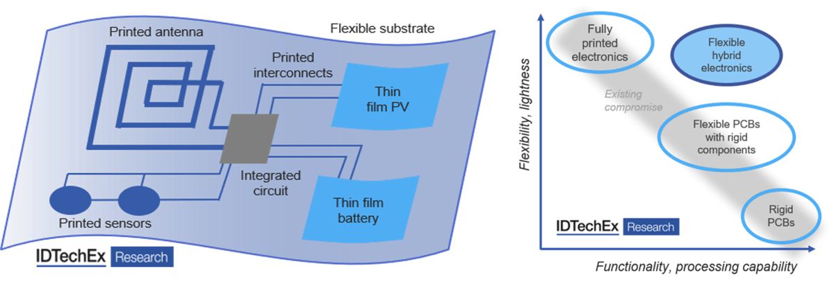
Additional functionality may include thin film photovoltaics (PV), a thin film battery and printed sensors. Schematic (right) showing how FHE breaks the existing compromise between processing capability and flexibility.
Flexible hybrid electronics (FHE) ends this compromise. It promises to combine the extensive processing capability of integrated circuits with a flexible form factor, and with printed rather than etched conductive interconnects. This combination of attributes opens a wide range of application possibilities, across many different industries. The new IDTechEx report finds that this could be a $3 Bn market by 2030.
Ubiquitous Electronics
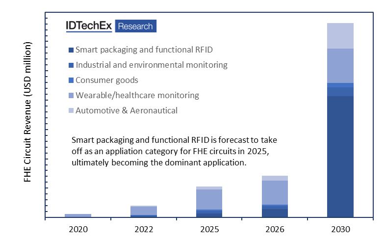
FHE provides a compelling technological approach towards the vision of ubiquitous electronics. The combination of flexibility, processing/communication capability and ultimately compatibility with low-cost, high volume continuous manufacturing methods is unique to FHE, but highly applicable to many different sectors. Their new FHE report identifies five main application sectors: smart packaging, wearable/healthcare monitoring, consumer electronics, industrial/environmental monitoring, and automotive/aeronautical.
RFID Sensors
Perhaps the most compelling opportunity for FHE is ubiquitous, low cost wirelessly enabled RFID sensors. These could be employed in industrial and environmental monitoring, and in smart packaging. Such capability is a prerequisite for the vision of connected devices and the ‘Internet of Things’, in which data from an increasingly wide range of items is transmitted to the cloud before applying machine learning. At present, passive RFID tags are produced by the billion. IDTechEx have been analyzing the RFID market research since the early 2000’s and estimate around 18 billion RFID tags will be produced in 2020 (see the IDTechEx report titled “RFID Forecasts, Players and Opportunities 2019-2029” for a complete analysis of the global RFID industry).
Passive RFID tags are only capable of communicating with a reader when specifically addressed. Furthermore, as the name suggests, their only functionality is identification. FHE would enable ‘RFID sensors’ that can monitor other attributes such as temperature, humidity, stress and strain at specified intervals, and then transmit that information either to a reader or via wireless networks.
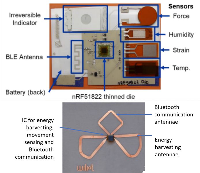
The picture below shows a prototype multimodal sensor from Boeing, which could be applied to industrial equipment large and small and would transmit information via Bluetooth to help predict equipment failure and thus improve productivity. Also shown is a prototype sensor from Wiliot, which has Bluetooth capability but does not include a thin film battery, instead harvesting electromagnetic energy from its surroundings. A battery-less approach seems a promising route to ubiquitous RFID sensors, since thin film batteries have limited capacity and will increase device size, cost and manufacturing complexity.
Innovative Thinned ICs
Such a vision will need such RFID sensors to be manufactured in very large volumes with a low cost per unit. This requires R2R (roll-to-roll manufacturing), which is currently employed for passive RFID tags. Adapting this method to FHE introduces some considerable challenges, since FHE circuits require a thinned die, and likely other passive components, to be mounted onto a flexible substrate.
Relative to basic RFID ICs that have very limited functionality, thinned FHE ICs (for example a module with ADC and UHF RFID measuring 2.2 mm by 2.3 mm by 25 um) have much higher aspect ratios and more I/O pads, increasing both fragility and registration requirements during placement. Differential thermal expansion coefficients between polymeric substrates and silicon ICs pose additional challenges for robust attachment, particularly if the circuit is going to be exposed to a wide range of temperatures, such as in automotive applications.
Given this challenge, the production, handling and attachment of thinned dies are very much an innovation area. IDTechEx forecast that RFID sensors will start becoming widely adopted in 2025, with over 5 billion units sold per year by 2030.
From PI to PET
The widespread adoption of RFID sensors requires them to be as cheap as possible. This precludes the use of expensive PI (polyimide) substrates, which will likely be replaced with PET (and even paper for smart packaging applications).
This transition in substrate materials imposes challenges, in that conventional lead-free (SnAgCu) solder can no longer be used. The development of component attachment methods that are compatible with thermally fragile substrates is an area of innovation, including both low temperature solder, novel anisotropic conductive adhesives, and photo-sintered solder.
An Opportunity for Conductive Ink
Conductive ink, required for the printed interconnects in an FHE circuit, provides another opportunity for cost reductions. Currently, most conductive ink is silver based, but are intrinsically expensive due to the price of silver metal (around 400 $/kg). Copper based inks are potentially much cheaper but have long suffered from unwanted oxidation that reduces conductivity. Developing stable copper inks with at least equivalent conductivity to silver inks, while reducing the curing times and temperatures to facilitate rapid manufacturing with thermally fragile substrates is thus a substantial area of innovation.
An elegant compromise
In summary, FHE is a new approach to electronic circuits that bridges the gap between printed and conventional electronics, by combining flexibility with processing capability, along with the potential for both agile and continuous manufacturing methods. This combination of attributes is ideally suited to applications including smart packaging, wearable devices and industrial/environmental monitoring. Challenges, and hence innovation areas, are transitioning to cheaper thermally fragile substrates and hence low temperature attachment methods, lowering the conductive ink, and making FHE circuit production compatible with R2R manufacturing.
IDTechEx’s new report, “Flexible Hybrid Electronics 2020-2030: Applications, Challenges, Innovations and Forecasts”, offers a comprehensive analysis of this emerging technology frontier. The analysts from IDTechEx have been assessing and following the printed electronic technologies and markets for well over a decade. This report is based on fresh primary research including interviews and company visits with all the key players worldwide.
It identifies and examines all the key innovation trends across the material and production systems, covering attachment, substrate, and metallization materials, as well as production techniques including high-throughput pick-and-place and various S2S and R2R printing techniques. This report builds an application roadmap, showing how FHE will grow in complexity from simple RFID tags of today to complex flexible hybrid electronics of the future, enabling applications in smart packaging, industrial monitoring and wearable devices and more. It offers insightful analysis into application timeline, challenges, and innovation opportunities.
Furthermore, it forecasts the growth of this enabling technology, showing that the market can exceed $3 bn by 2030. Smart packaging is forecast to be the dominant application by volume, although wearable/healthcare monitoring applications are likely to be first to achieve significant market penetration.