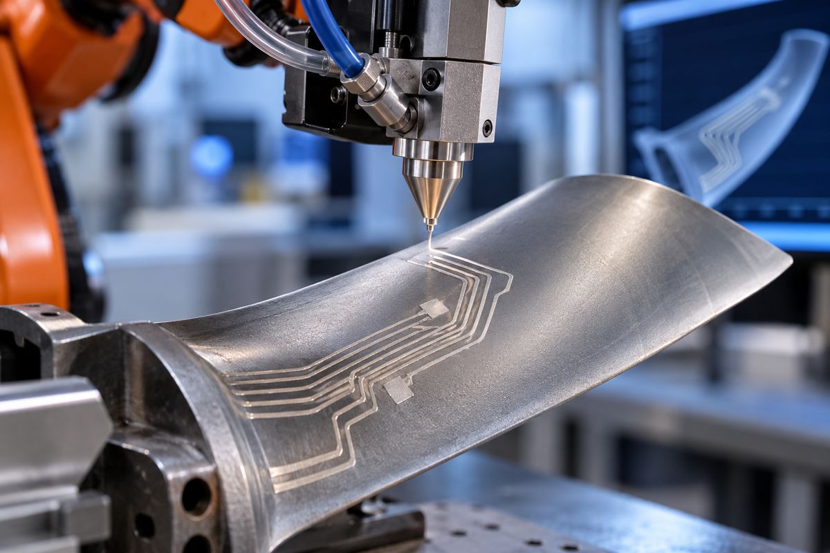







Semiconductor created using Graphene opens door on a new era in Electronics
Researchers at the Georgia Institute of Technology have created the world’s first functional semiconductor made from graphene, a single sheet of carbon atoms held together by the strongest bonds known. Semiconductors, which are materials that conduct electricity under specific conditions, are foundational components of electronic devices. The team’s breakthrough throws open the door to a new way of doing electronics.
Their discovery comes at a time when silicon, the material from which nearly all modern electronics are made, is reaching its limit in the face of increasingly faster computing and smaller electronic devices. Walter de Heer, Regents’ Professor of physics at Georgia Tech, led a team of researchers based in Atlanta, Georgia, and Tianjin, China, to produce a graphene semiconductor that is compatible with conventional microelectronics processing methods — a necessity for any viable alternative to silicon.
In this latest research, published in Nature, de Heer and his team overcame the paramount hurdle that has been plaguing graphene research for decades, and the reason why many thought graphene electronics would never work. Known as the “band gap,” it is a crucial electronic property that allows semiconductors to switch on and off. Graphene didn’t have a band gap — until now.
“We now have an extremely robust graphene semiconductor with 10 times the mobility of silicon, and which also has unique properties not available in silicon,” de Heer said. “But the story of our work for the past 10 years has been, ‘Can we get this material to be good enough to work?’”
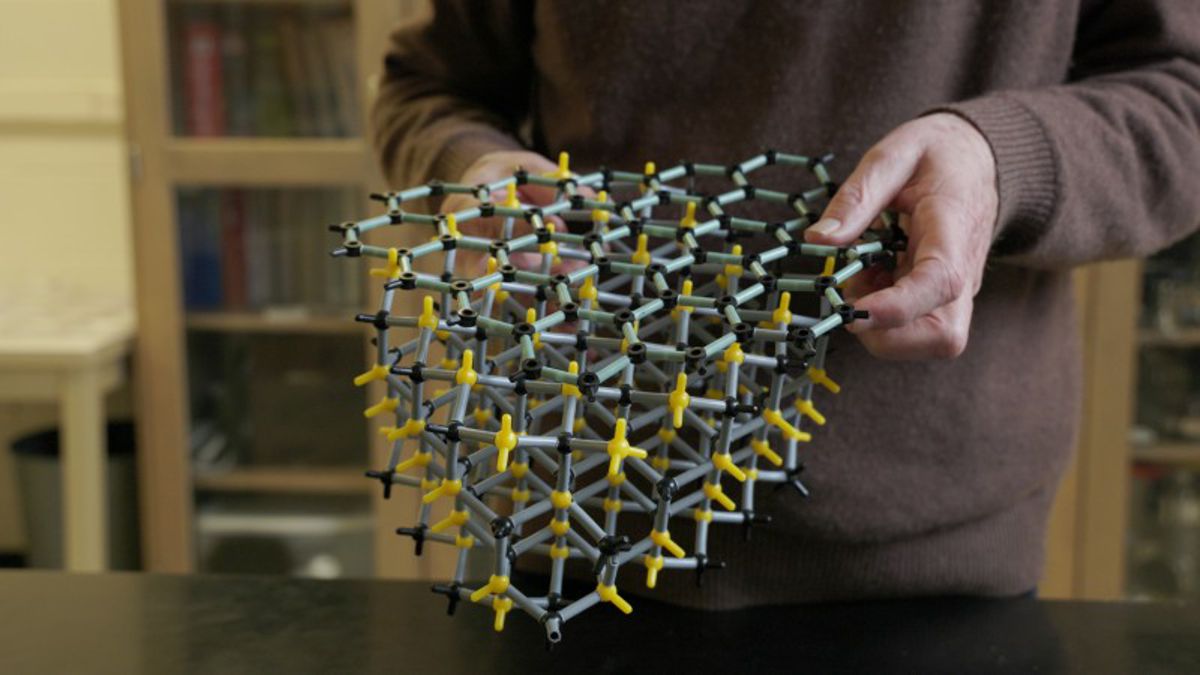
A New Type of Semiconductor
De Heer started to explore carbon-based materials as potential semiconductors early in his career, and then made the switch to exploring two-dimensional graphene in 2001. He knew then that graphene had potential for electronics.
“We were motivated by the hope of introducing three special properties of graphene into electronics,” he said. “It’s an extremely robust material, one that can handle very large currents, and can do so without heating up and falling apart.”
De Heer achieved a breakthrough when he and his team figured out how to grow graphene on silicon carbide wafers using special furnaces. They produced epitaxial graphene, which is a single layer that grows on a crystal face of the silicon carbide. The team found that when it was made properly, the epitaxial graphene chemically bonded to the silicon carbide and started to show semiconducting properties.
Over the next decade, they persisted in perfecting the material at Georgia Tech and later in collaboration with colleagues at the Tianjin International Center for Nanoparticles and Nanosystems at Tianjin University in China. De Heer founded the center in 2014 with Lei Ma, the center’s director and a co-author of the paper.

How They Did It
In its natural form, graphene is neither a semiconductor nor a metal, but a semimetal. A band gap is a material that can be turned on and off when an electric field is applied to it, which is how all transistors and silicon electronics work. The major question in graphene electronics research was how to switch it on and off so it can work like silicon.
But to make a functional transistor, a semiconducting material must be greatly manipulated, which can damage its properties. To prove that their platform could function as a viable semiconductor, the team needed to measure its electronic properties without damaging it.
They put atoms on the graphene that “donate” electrons to the system — a technique called doping, used to see whether the material was a good conductor. It worked without damaging the material or its properties.

The team’s measurements showed that their graphene semiconductor has 10 times greater mobility than silicon. In other words, the electrons move with very low resistance, which, in electronics, translates to faster computing. “It’s like driving on a gravel road versus driving on a freeway,” de Heer said. “It’s more efficient, it doesn’t heat up as much, and it allows for higher speeds so that the electrons can move faster.”
The team’s product is currently the only two-dimensional semiconductor that has all the necessary properties to be used in nanoelectronics, and its electrical properties are far superior to any other 2D semiconductors currently in development.
“A long-standing problem in graphene electronics is that graphene didn’t have the right band gap and couldn’t switch on and off at the correct ratio,” said Ma. “Over the years, many have tried to address this with a variety of methods. Our technology achieves the band gap, and is a crucial step in realizing graphene-based electronics.”
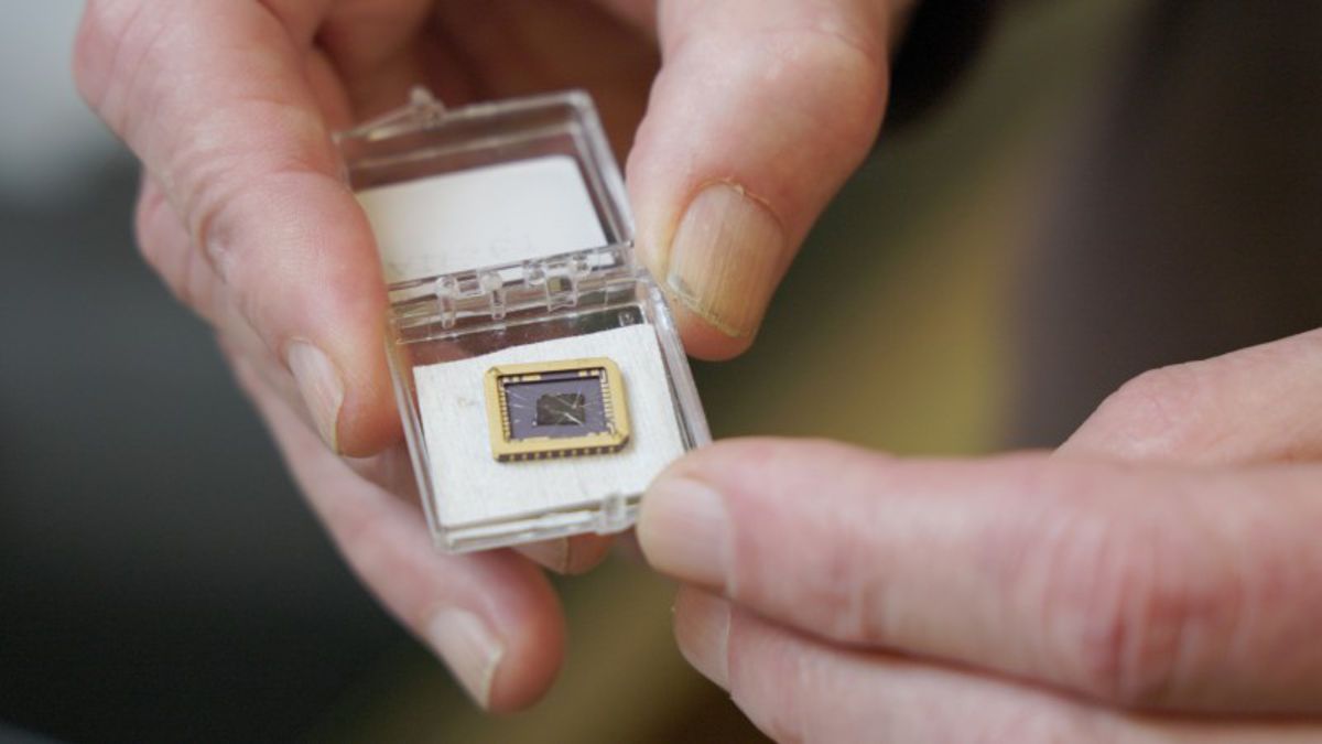
Moving Forward
Epitaxial graphene could cause a paradigm shift in the field of electronics and allow for completely new technologies that take advantage of its unique properties. The material allows the quantum mechanical wave properties of electrons to be utilized, which is a requirement for quantum computing.
“Our motivation for doing graphene electronics has been there for a long time, and the rest was just making it happen,” de Heer said. “We had to learn how to treat the material, how to make it better and better, and finally how to measure the properties. That took a very, very long time.”

According to de Heer, it is not unusual to see yet another generation of electronics on its way. Before silicon, there were vacuum tubes, and before that, there were wires and telegraphs. Silicon is one of many steps in the history of electronics, and the next step could be graphene.
“To me, this is like a Wright brothers moment,” de Heer said. “They built a plane that could fly 300 feet through the air. But the skeptics asked why the world would need flight when it already had fast trains and boats. But they persisted, and it was the beginning of a technology that can take people across oceans.”