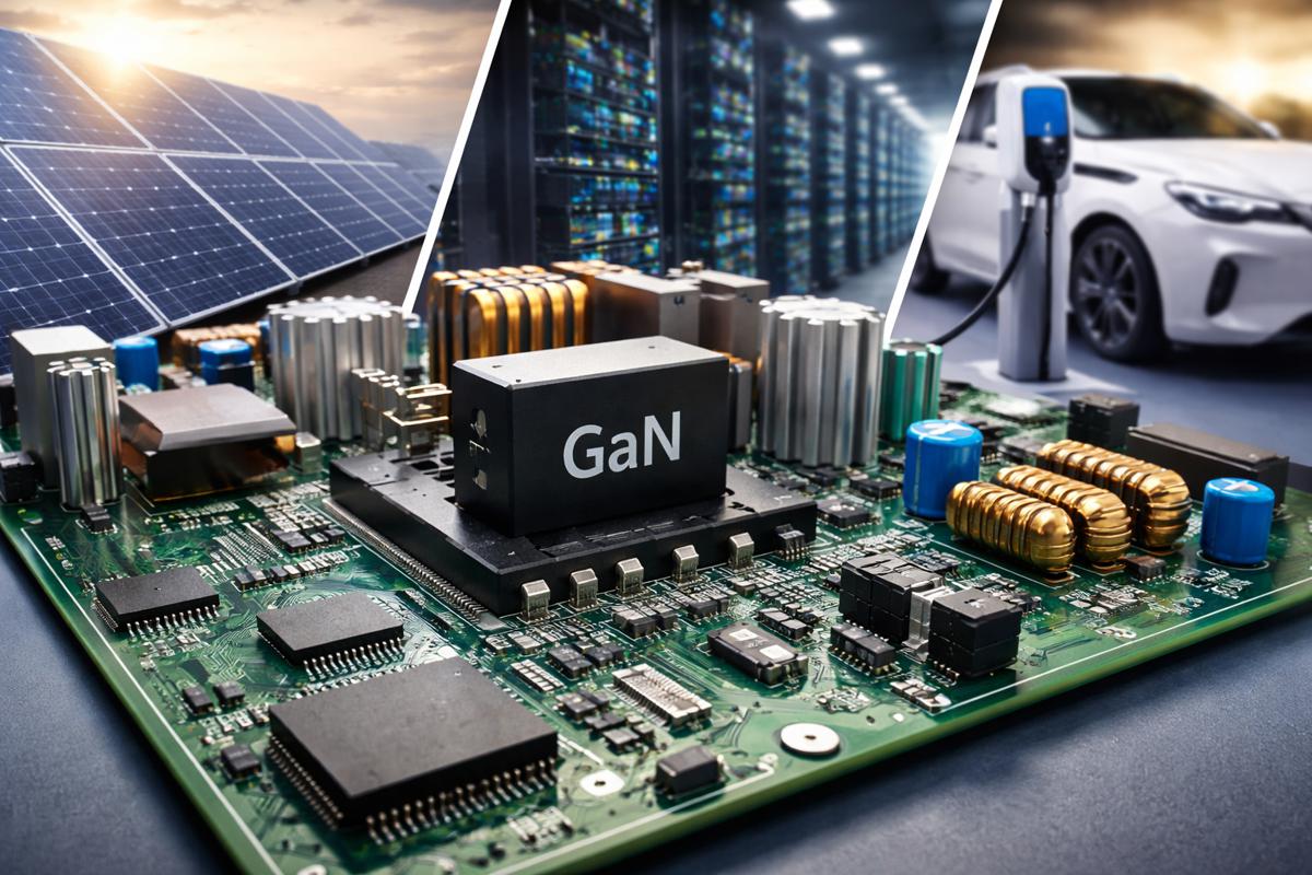


GaN Power Breakthrough Reshapes Energy Conversion
Power conversion has long sat quietly at the heart of modern infrastructure, yet its influence stretches across everything from solar farms and transport electrification to hyperscale data centres. Now, a significant leap in gallium nitride technology is beginning to redraw the design rules that engineers have worked around for decades.
Renesas Electronics Corporation has introduced two complementary advances that, taken together, signal a decisive shift in how power systems will be designed, scaled and deployed. At the centre of this development is the industry’s first bidirectional depletion mode GaN switch, alongside a new high power Half Wave LLC converter platform. Both are aimed squarely at sectors where efficiency, compactness and thermal control are no longer optional extras but hard commercial requirements.
The implications go well beyond component-level innovation. By simplifying architectures and improving performance, these technologies open the door to more efficient renewable energy systems, denser data infrastructure and faster, more practical electrification of transport. In short, they address the bottlenecks that have quietly constrained progress across multiple infrastructure domains.
Breaking the Limits of Conventional Switching Architectures
Traditional power conversion has relied heavily on silicon and silicon carbide switches that operate in a fundamentally unidirectional manner. While effective, this limitation forces engineers into multi stage conversion architectures, often involving multiple switching bridges, intermediate DC links and a significant increase in component count.
In practical terms, that complexity comes at a cost. More components mean higher losses, larger footprints, increased thermal management challenges and ultimately reduced system efficiency. Solar microinverters, for example, have typically required two separate conversion stages, each introducing its own inefficiencies and design constraints.
Renesas’ new bidirectional GaN device changes that equation. By enabling current blocking in both directions within a single component, it removes the need for back to back switching arrangements. The result is a shift towards true single stage conversion, where fewer components can deliver higher efficiency and improved reliability.
This is not just an incremental improvement. It represents a structural simplification of power electronics design, allowing engineers to rethink system architectures rather than merely optimise existing ones.
Efficiency Gains That Matter at System Scale
At first glance, a marginal increase in efficiency might seem modest. However, when applied across large scale infrastructure systems, even small gains translate into significant operational savings and reduced environmental impact.
In real world testing, single stage solar microinverter designs using the new GaN architecture have demonstrated efficiency levels exceeding 97.5 percent. That figure is notable not only because it surpasses many conventional designs, but because it is achieved while simultaneously reducing component count and eliminating intermediate energy storage elements.
Across solar installations, such improvements can increase overall energy yield and reduce balance of system costs. In data centres, where power conversion losses directly impact operating expenditure and cooling requirements, higher efficiency contributes to both cost savings and sustainability targets. Meanwhile, in electric vehicle onboard chargers, improved efficiency extends driving range and reduces charging times, addressing two of the most persistent barriers to wider EV adoption.
Global trends reinforce the importance of such gains. According to the International Energy Agency, data centre electricity demand is projected to grow significantly through the decade, while electrification of transport continues to accelerate. Against that backdrop, more efficient power conversion is not just desirable but essential.
Simplifying Design Without Sacrificing Performance
One of the persistent challenges with advanced semiconductor technologies has been the trade off between performance and usability. High performance devices often require complex control schemes, specialised drivers or additional circuitry, offsetting some of their theoretical advantages.
Renesas has taken a different approach with its SuperGaN technology. By using a depletion mode architecture in a cascode configuration, the device maintains compatibility with standard silicon gate drivers. This eliminates the need for negative gate bias and simplifies the overall gate drive design.
In practical engineering terms, that translates to faster development cycles, reduced design risk and lower system cost. Engineers can integrate the new device into existing design frameworks without having to overhaul their entire control strategy.
At the same time, the device delivers high switching speeds, strong dv dt immunity exceeding 100 volts per nanosecond and robust operation under both soft and hard switching conditions. These characteristics make it suitable for demanding topologies such as Vienna rectifiers, which are commonly used in industrial and data centre applications.
As Rohan Samsi, Vice President of Renesas’ GaN Business Division, explained: “Extending our SuperGaN technology to the bidirectional GaN platform marks a major shift in power conversion design norms. Customers can now achieve higher efficiency with fewer switching components, smaller PCB area and lower system cost. At the same time, they can accelerate design by leveraging Renesas’ system-level integration with gate drivers, controllers and power management ICs.”
Scaling Power Delivery for a High Demand World
Alongside its bidirectional switch, Renesas has expanded its AC DC power portfolio with a Half Wave LLC converter platform designed to scale well beyond traditional limits. Historically, LLC converters have been widely used in the 100 watt range, particularly for consumer electronics and smaller power supplies.
The new platform extends that capability to 500 watts and beyond, opening up new applications across industrial systems, infrastructure equipment and high power consumer devices. This includes large displays, industrial lighting, power tools and fast charging systems for e mobility solutions.
At the heart of this development is a coordinated ecosystem of controller ICs, including an interleaved power factor correction and resonant conversion controller. By integrating these functions, the system reduces ripple, balances current and improves overall efficiency while maintaining a compact form factor.
The introduction of USB Extended Power Range, supporting up to 240 watts, is particularly significant. It reflects a broader industry shift towards standardised, high power charging solutions that can replace proprietary adapters. In practical terms, this could reduce electronic waste, simplify device ecosystems and improve user convenience.
Jenny Ng, General Manager of Belkin Asia, highlighted the real world impact of this approach: “The Belkin Z-Charger is a major step toward a new era of ultra-low standby power consumption in fast charging.”
GaN as a Foundation for Power Density and Thermal Control
The underlying driver of these advances is gallium nitride itself. Compared with silicon, GaN offers higher electron mobility, enabling faster switching speeds and lower losses. These characteristics allow designers to reduce the size of passive components such as transformers and inductors, which traditionally dominate the physical footprint of power systems.
In the context of infrastructure, higher power density is more than a technical achievement. It enables more compact installations, reduces material usage and simplifies integration into constrained environments such as electric vehicles or urban infrastructure systems.
Thermal performance is equally critical. By reducing switching losses and improving efficiency, GaN based systems generate less heat, easing cooling requirements and improving reliability. This is particularly important in applications such as data centres and industrial equipment, where thermal management can account for a significant portion of total system cost.
The new Half Wave LLC platform builds on these advantages by reducing transformer complexity and component count. This not only improves efficiency but also simplifies manufacturing and supply chain management, an increasingly important consideration in a world of volatile component availability.
From Component Innovation to Infrastructure Impact
The broader significance of these developments lies in their cumulative effect. Individually, a more efficient switch or a higher power converter might appear as incremental improvements. Together, they represent a step change in how power systems can be designed and deployed.
For renewable energy, simpler and more efficient conversion supports higher penetration of distributed generation. For transport, it accelerates the shift towards electrification by improving charging infrastructure and onboard systems. For digital infrastructure, it enables the continued expansion of data capacity without proportional increases in energy consumption.
At a time when global infrastructure is under pressure to become more sustainable, resilient and efficient, such advances are not merely technical milestones. They are enablers of broader systemic change.
A More Efficient Future for Power Conversion
As power demands continue to rise across sectors, the need for smarter, leaner and more efficient conversion technologies becomes increasingly urgent. The combination of bidirectional GaN switching and scalable high power conversion platforms offers a glimpse of what that future could look like.
By reducing complexity, improving efficiency and enabling higher power density, these innovations provide engineers with new tools to meet the challenges of modern infrastructure. The result is not just better performance at the component level, but a more efficient and adaptable energy ecosystem overall.