


Flawed diamonds can lead to flawless quantum networks
The colour in a diamond comes from a defect, or “vacancy,” where there is a missing carbon atom in the crystal lattice. Vacancies have long been of interest to electronics researchers because they can be used as ‘quantum nodes’ or points that make up a quantum network for the transfer of data. One of the ways of introducing a defect into a diamond is by implanting it with other elements, like nitrogen, silicon, or tin.
In a recent study published in ACS Photonics, scientists from Japan demonstrate that lead-vacancy centres in diamond have the right properties to function as quantum nodes.
“The use of a heavy group IV atom like lead is a simple strategy to realize superior spin properties at increased temperatures, but previous studies have not been consistent in determining the optical properties of lead-vacancy centres accurately,” says Associate Professor Takayuki Iwasaki of Tokyo Institute of Technology (Tokyo Tech), who led the study.
The three critical properties researchers look for in a potential quantum node are symmetry, spin coherence time, and zero phonon lines (ZPLs), or electronic transition lines that do not affect “phonons,” the quanta of crystal lattice vibrations. Symmetry provides insight into how to control spin (rotational velocity of subatomic particles like electrons), coherence refers to an identicalness in the wave nature of two particles, and ZPLs describe the optical quality of the crystal.
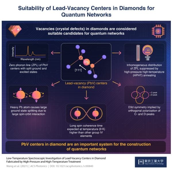
The researchers fabricated the lead-vacancies in diamond and then subjected the crystal to high pressure and high temperature. They then studied the lead vacancies using photoluminescence spectroscopy, a technique that allows you to read the optical properties and to estimate the spin properties. They found that the lead-vacancies had a type of dihedral symmetry, which is appropriate for the construction of quantum networks.
They also found that the system showed a large “ground state splitting,” a property that contributes to the coherence of the system. Finally, they saw that the high-pressure high-temperature treatment they inflicted upon the crystals suppressed inhomogeneous distribution of ZPLs by recovering the damage done to the crystal lattice during the implantation process. A simple calculation showed that lead-vacancies had a long spin coherence time at a higher temperature (9K) than previous systems with silicon and tin vacancies.
“The simulation we presented in our study seems to suggest that the lead-vacancy centre will likely be an essential system for creating a quantum light-matter interface—one of the key elements in the application of quantum networks,” concludes an optimistic Dr. Iwasaki.
This study paves the way for the future development of large (defective) diamond wafers and thin (defective) diamond films with reliable properties for quantum network applications.